

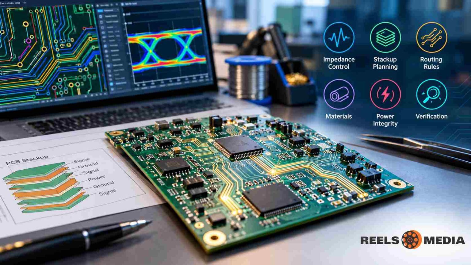
A PCB is a high speed design when signal edges are fast enough that the copper traces behave like transmission lines instead of simple wires. This depends on rise time, not clock frequency. A 10 MHz clock with a 500 ps edge needs more care than a 200 MHz signal with a slow edge.
This guide covers the engineering methods behind high speed PCB design Radiocord technologies, meaning impedance control, stackup, routing, materials, power integrity and verification. It makes no claims about any specific company’s products or services.
When Does a Board Become High Speed?
Use rise time to decide. Two quick calculations cover most cases:
- Knee frequency: about 0.35 divided by the rise time. A 1 ns edge has significant energy up to roughly 350 MHz. A 100 ps edge reaches about 3.5 GHz.
- Critical length: a trace needs transmission line treatment when its delay exceeds roughly one sixth of the rise time. In FR4, signals travel at about half the speed of light, which is around 150 to 180 ps per inch depending on whether the trace is on an outer or inner layer. A 1 ns edge makes any trace longer than about 1 inch worth checking.
Fast edges are common even in modest products. Many microcontrollers, DDR memory, USB, PCIe, Ethernet, HDMI, MIPI and SerDes links all need these rules.
Controlled Impedance
A signal that meets a sudden impedance change reflects part of its energy back. The result is ringing, overshoot and eye diagram closure. Controlled impedance keeps the trace’s characteristic impedance steady from driver to receiver.
Typical targets (always confirm against the interface specification and the chip datasheet):
| Interface | Common target |
| General single-ended signals | 50 ohm |
| USB 2.0 and 3.x differential pairs | 90 ohm |
| Ethernet, LVDS, HDMI, many SerDes | 100 ohm differential |
| PCIe | 100 ohm differential, with some designs using 85 ohm |
| DDR memory | Varies by generation, often 40 to 50 ohm single-ended |
Impedance depends on trace width, copper thickness, dielectric thickness and dielectric constant. Change any of these and the number moves. A field solver gives far better results than online formulas, especially for differential pairs and coplanar structures.
Standard fabrication tolerance is usually ±10%. Tighter control, such as ±5%, is possible but may cost more. Fabricators adjust trace width slightly to hit your target, so send them the target impedance and the layers it applies to, not just a trace width.



Stackup Planning
Decide the stackup before routing. Every fast signal needs a continuous reference plane directly next to it.
A common 6-layer arrangement:
- Top: signals and components
- Ground plane
- Inner signal layer (stripline)
- Power plane
- Ground plane
- Bottom: signals and components
Layer 3 sits between ground and power, so keep the power plane quiet and tightly coupled to its neighboring ground. Thin dielectrics between signal and reference layers give lower impedance for a given trace width, tighter coupling and less crosstalk.
If two signal layers sit next to each other, route them at right angles to limit broadside coupling. Keep the stackup symmetrical around the center to reduce warpage during assembly.
Routing Rules That Matter Most
Protect the return path
Current returns to the source underneath the trace, on the nearest reference plane. If the plane has a slot, split or gap, the return current detours and creates loop area. That means more radiation, more crosstalk and a noisier signal. Never route a fast signal across a plane split.
Handle layer changes carefully
When a signal changes layers and the reference plane changes too, the return current needs a path between the planes. Place a ground stitching via within a few millimeters of the signal via. For differential pairs, put one on each side.
Reduce via damage
Vias add capacitance and inductance. A through-hole via that connects top to an inner layer leaves an unused stub, which can resonate at high frequencies. At multi-gigabit speeds, use back drilling, blind or buried vias, or route on layers that keep the stub short. At lower speeds, keeping via counts down is usually enough.
Differential pair discipline
- Keep both traces the same length and the same distance apart along their whole run.
- Match length within each pair first, then between pairs where the protocol requires it.
- Add length tuning near the source of the mismatch, not at the end of the route.
- Avoid sharp corners. Use 45-degree bends or smooth arcs.
Crosstalk control
Spacing is the main defense. The 3W rule, which puts trace centers three trace widths apart, is a useful starting point, not a guarantee. Aggressive signals such as clocks need more. Parallel runs over long distances are the real problem, so shorten them where you can. Guard traces only help when they are grounded frequently with vias. A floating guard trace can make things worse.
Length matching for parallel buses
DDR byte lanes, for example, require data lines to match their strobe within tight limits set by the memory standard. Follow the chip vendor’s routing guidelines, since the limits differ between DDR generations.
Materials: FR4 and Beyond
FR4 works for many high speed designs, especially below a few gigabits per second on short traces. Its weakness is loss. Standard FR4 has a dissipation factor around 0.02, and that loss grows with frequency and trace length.
Two material effects deserve attention:
- Dielectric loss: low-loss laminates (dissipation factor below about 0.01, with premium grades much lower) are used for long channels at 10 Gbps and above. Panasonic Megtron, Isola and Rogers families are well-known examples.
- Fiber weave effect: the glass cloth in FR4 is uneven, so one trace of a differential pair may run over glass while the other runs over resin. They then see different dielectric constants and arrive at slightly different times. Spread-glass laminates or slightly angled routing reduce this.
Copper surface roughness also adds loss at high frequency. Smooth copper foil helps in demanding channels.
A quick selection guide: if the board has short traces and data rates under about 5 Gbps, test FR4 first. If channel loss budgets get tight, move to a low-loss material before spending weeks tuning layout.
Power Integrity
Fast switching pulls sharp current spikes from the power network. If the supply impedance is too high, voltage dips and noise appear on the rails, and they show up as jitter on your signals.
- Target impedance: allowed voltage ripple divided by transient current. Design the power network to stay below this across the frequency range.
- Decoupling: place small-value capacitors as close to the power pins as possible, with short, wide connections to the plane. Capacitor loop inductance matters more than capacitor value at high frequency.
- Plane pairs: closely spaced power and ground planes act as a free high-frequency capacitor.
- Mixed values: use several capacitor values to cover a wider frequency range, but check the result in simulation rather than relying on a fixed recipe.
Verification: Simulate, Fabricate, Measure
Pre-layout simulation checks topology and termination choices. Post-layout simulation checks the real traces, vias and connectors. Commonly used tools include Cadence Sigrity and Allegro, Keysight ADS, Ansys HFSS and SIwave, Siemens HyperLynx, and Altium’s built-in analysis. For impedance only, a dedicated field solver is enough.
For fabrication, ask for:
- impedance test coupons on the panel
- a stackup drawing approved before layout
- a TDR (time-domain reflectometry) report for controlled-impedance nets
After assembly, measure with an oscilloscope, a TDR or a vector network analyzer, depending on what you need to prove. Compliance tests for USB, PCIe or Ethernet check eye diagrams and jitter against the standard’s limits.
Common Mistakes
- Choosing the stackup after routing is finished
- Routing across split planes or plane gaps
- Forgetting ground vias near layer transitions
- Using a single trace-width calculator result without a field solver or fabricator confirmation
- Matching differential pair length while ignoring skew caused by routing around obstacles
- Placing decoupling capacitors far from the pins and connecting them with long thin traces
- Treating connector footprints as ideal, when pad and antipad geometry can create large impedance bumps
- Skipping simulation because the data rate “seems low”, then discovering fast edge rates on a modern chip
Frequently Asked Questions (FAQs)
What frequency makes a PCB “high speed”?
No fixed frequency defines it. Rise time matters more than clock speed. If a trace’s delay exceeds about one sixth of the signal’s rise time, it should be treated as a transmission line. In FR4, that means traces longer than roughly an inch can need attention when edges are around 1 ns.
Can standard FR4 be used for high speed PCB design?
Yes, for many designs. It works well on short traces and data rates up to a few gigabits per second. For long channels at 10 Gbps and above, FR4’s dielectric loss and weave effect often push designers toward low-loss laminates.
What impedance values are most common?
The usual targets are 50 ohm single-ended and 90 to 100 ohm differential. USB uses 90 ohm differential, while Ethernet, LVDS and HDMI commonly use 100 ohm. Always confirm the exact value in the interface specification and chip datasheet.
How many layers does a high speed board need?
Most designs need at least four layers so each fast signal has a solid reference plane next to it. Six layers give more routing room and better power integrity. Two-layer boards only suit slow edges and short traces.
How do I reduce crosstalk on a high speed PCB?
Increase spacing between parallel traces, keep parallel runs short, and place signals close to their reference plane. The 3W rule (center-to-center spacing of three trace widths) is a starting point. Aggressive signals like clocks need more. Grounded guard traces help only if they are stitched with vias frequently.
Is simulation necessary for every high speed design?
Not always. Low-risk designs that follow the chip vendor’s layout guidelines may not need full simulation. Multi-gigabit links, DDR memory and designs with long channels, many connectors or tight margins benefit most, because simulation catches problems before fabrication costs are spent.
Conclusion
High speed PCB design Radiocord technologies, as a discipline, comes down to a few decisions made early: define the stackup, hit the impedance target, protect the return path, and choose a material that fits your loss budget. Get those right and simulation becomes a confirmation step instead of a rescue operation. Always check interface specifications and datasheets for exact values, because limits change between standards and generations.